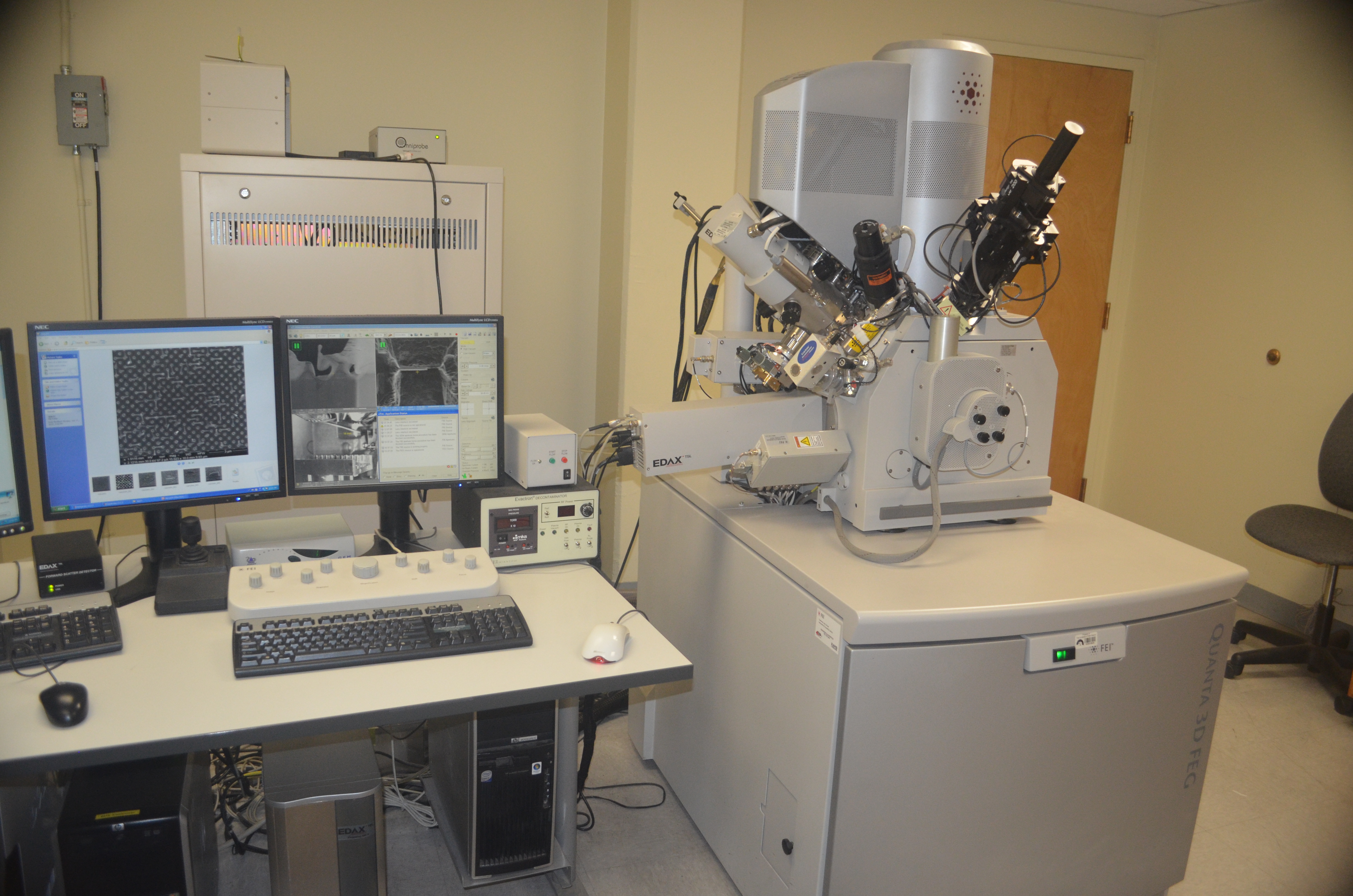
Quanta 3D FEG
 The FEI Quanta 3D is a dual-beam (SEM/FIB) system with both e-beam mode and ion-beam mode. Besides all functions for a standard SEM, the Q3D is also capable using ion beam to form images and cut samples.
The capabilities of this system include:
SEM Mode Functions:
- Regular SEM functions including both SE and BSE images, with 3.0nm resolution at 30 kV
- Low vacuum SEM mode the allows existence of moderate moisture in the chamber for improved conductivity without Au coating
- Back scattered electron diffraction (BSED) to analyze crystal structures and map crystal type, grain size, as well as crystal orientations
- EDS spectrum and EDS mapping
Unique SEM Functions:
- Extended low vacuum SEM mode (ESEM, environmental SEM mode) that allows introduction of external gases (e.g. water vapor)
- High-temperature SEM mode up to 800 <sup>o</sup>C with heated sample stage
- E-beam lithography
- E-beam assisted deposition of Pt, or W. (a pattern can be defined or uploaded and the Pt- or W- deposition will follow the pattern as defined.)
FIB mode Functions:
- Regular ion-beam imaging using SE detector with 7 nm resolution at 30 kV
- Advantages of e-beam image: 1) use smaller current than e-beam, reduced charging issue; 2) strong contract in channeling effect, with better contract in grain orientations.
- Cutting trenches or patterns with FIB (a pattern can be defined or uploaded and the Pt- or W- deposition will follow the pattern as defined.)
- Ion beam assisted Platinum deposition (a pattern can be defined or uploaded and the Pt- or W- deposition will follow the pattern as defined.)
- Ion beam assisted Tungsten deposition (a pattern can be defined or uploaded and the Pt- or W- deposition will follow the pattern as defined.)
- FIB sectioning for in situ SEM cross-section
- FIB sectioning for TEM sample prep.
Examples of nanofabrication capabilities:
- Fabrication of nanowire-based or nanotube-based devices, e.g. to measure electron current through a nanowire;
- Fabrication of micron-/nano- trench based devices such as nanofluidic devices
- E-beam lithography
- Fabrication of grating or prototype mask
- AFM tip modification
- Photonic or phononic array fabrication
- Nano stamping
- MEMS modification and wiring
- In situ repair of microelectronic devices
E-beam Optics:
- Electron Source: FEG,
- Accelerating voltage: 30 kV
- Beam current: to 20 nA in 21 steps
- Max Field of view: (the width of the largest area to see at lowest mag)
Detectors and Attachments:
- Everhardt-Thornley SED
- Low-vacuum SED (used in low vacuum)
- Gaseous SED (GSED) (used in ESEM mode)
- Solid-State BSED
- Gaseous analytical BSED (GAD) (used for low-vacuum analytical applications)
- EDS: Oxford silicon drift detector (50 mm<sup>2</sup>) and INCA software
- HKL EBSD (Electron Backscatter Diffraction) systems
E-beam Optics:
- Ion beam Source:Ga LMIS (liquid metal ion source)
- Accelerating voltage: 30 kV
- Beam current: 2 pA to 65 nA in 15 steps
- Max Field of view: (the width of the largest area to see at lowest mag)
Sample stage capability:
- Fits large sample: 1.5 x 3.0 400m
- samples size, or larger if no rotation is needed.
- Max movement of sample stage: X = + - 20 mm; Y = + - 40 mm
- Stage Tilt angle: -20 degrees to + 75 degrees
Location
Northrop Hall Room B06
Scheduling
To schedule time on this instrument or to learn more about its capabilities and user fees, etc. please contact:
Adrian Brearley
Distinguished Professor, Earth and Planetary Sciences
Director, Nanomaterials Characterization Facility
505 507 0448
brearley@unm.edu